
Case Study
Tech deep dive: wide‑bandgap devices supply chains from mine to module: Latest Developments and

Tech Deep Dive: Wide‑Bandgap Devices Supply Chains from Mine to Module
Wide‑bandgap (WBG) semiconductors based on gallium nitride (GaN) and silicon carbide (SiC) have moved from niche to system‑defining in less than a decade. They now sit at the heart of EV traction inverters, fast chargers, 5G base stations, AI data center power supplies, and radar and electronic warfare systems. Market analysis from SkyQuest projects the GaN/SiC power semiconductor segment will grow from roughly $3.63 billion in 2025 to $22.48 billion by 2033, implying a compound annual growth rate above 25% [7].
This pace of deployment collides with a supply chain that was never designed for strategic scale. Gallium is largely a byproduct of alumina and zinc refining, not a primary mined commodity; SiC begins with metallurgical‑grade silicon and carbon in highly energy‑intensive furnaces; and the transition from 150 mm to 200 mm and ultimately 300 mm substrates magnifies defect sensitivity at every step. Export controls, carbon policies, and forced labor regulations further complicate sourcing strategies.
Structured differently from silicon logic, the WBG stack concentrates technical and geopolitical risk in a handful of upstream and midstream nodes-particularly refined gallium and high‑purity SiC substrates-while downstream module assembly remains comparatively flexible. Understanding this asymmetry is critical for any OEM, Tier‑1, or government agency relying on WBG devices for electrification and digital infrastructure.
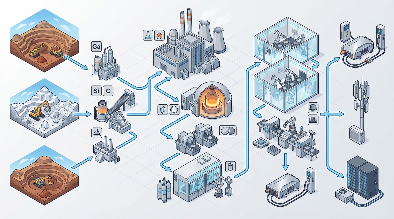
This deep dive traces the WBG chain from mine to module, focusing on gallium and SiC raw materials, substrate and epi capacity, wafer fabrication, and final module integration. It emphasizes operational chokepoints for the 2024-2033 period: where supply concentration is highest, where scaling physics is most unforgiving, and where regulatory moves can instantaneously reprice technical roadmaps.
1. Upstream Materials: Gallium, Silicon and Carbon as Strategic Precursors
For GaN, the critical mineral is gallium; for SiC, the critical precursors are high‑purity silicon and carbon. Unlike copper or nickel, these WBG feedstocks are not typically mined as primary products. Gallium is recovered from Bayer liquor in alumina refineries and from zinc process streams; silicon comes from quartzite reduction; and carbon is often petroleum‑based coke or coal‑derived. This byproduct character structurally limits supply elasticity.
USGS reporting and IEA critical mineral assessments both underline gallium’s concentration risk, with China historically accounting for the overwhelming majority of refined primary gallium output, well above 90% of the global total. Market work cited in Deloitte’s GaN/SiC overview and other sources approximates current gallium production around 500 metric tonnes per year, with the bulk originating from a very small number of alumina and zinc smelters [2].
1.1 Gallium from Bauxite and Zinc: Process and Geography
In the Bayer process for alumina, bauxite is digested in caustic soda at high temperature and pressure, dissolving alumina and co‑dissolving trace gallium. Gallium accumulates in the spent liquor over multiple cycles. Recovery typically involves cementation (using aluminum metal to displace gallium), solvent extraction, and electrolysis or distillation to produce crude gallium metal. Further refining (often multiple passes of zone refining) yields 4N-6N purity feedstock for GaN epitaxy.
Operationally, gallium recovery layers new unit operations on legacy alumina flowsheets: solvent extraction mixers, electrolytic cells, high‑temperature distillation columns, and zone‑refining furnaces. These stages consume electricity and reagents but, more importantly, require tight process control to avoid contaminating gallium with sodium, iron, or other metallic impurities that would degrade GaN epitaxial quality.
On the ground, a few facilities dominate:
- Jinchuan Group and associated refineries in China (e.g., Gansu, Inner Mongolia): Integrated with large alumina operations that process bauxite from Bayan Obo and other deposits, these facilities are frequently cited as controlling a substantial share of global refined gallium output. Industry analysis referenced in [2] and [9] attributes around 30% of world gallium production to Jinchuan alone and indicates material is upgraded to roughly 4N purity for downstream GaN substrate producers, including Japanese and global customers.
- ENRC (Eurasian Resources Group) assets in Kazakhstan: Gallium is recovered as a byproduct from aluminum smelting, with public expansion plans targeting incremental capacity in the mid‑2020s. Logistics via the Caspian and Black Seas create routing exposure to geopolitical disruptions and maritime chokepoints.
- Additional gallium streams from Europe and Russia: Smaller refineries in France and Russia contribute non‑trivial volumes but remain constrained by aging smelter infrastructure and, in Russia’s case, by sanctions and financing restrictions.
China’s July 2023 export licensing regime on gallium and germanium already illustrated how policy can reprice WBG devices. Scenario analysis in sources such as [9] explores potential next steps, including formal export quotas or tighter end‑use controls post‑2025. In modeled cases where non‑aligned exports are capped, spot gallium prices are projected to spike substantially—some scenarios cite levels around $1,200/kg by 2026—before stabilizing once alternative recovery lines ramp.
From an operational risk standpoint, a single export licensing decision in Beijing can now propagate through epitaxy lines in Japan, substrates in Europe, and EV inverter production in North America within one model year. That linkage between alumina byproduct policy and traction inverter availability is structurally new.
1.2 Silicon and Carbon Streams for SiC
SiC begins with metallurgical‑grade silicon (MG‑Si) and carbon, typically produced via carbothermal reduction of high‑purity quartz in submerged‑arc furnaces. The classical Acheson or similar processes operate at temperatures above 2,000 °C, drawing substantial electrical power. The output is a mix of SiC and byproducts that undergo crushing, classification, and further refining steps.
Upgrading to semiconductor‑grade SiC requires progressively tighter impurity control. Metallic contaminants (Fe, Al, Ti), oxygen, and nitrogen must be reduced to very low ppm or ppb levels, depending on target device breakdown voltage and lifetime. This upgrade typically relies on combinations of high‑temperature recrystallization, chemical vapor deposition (CVD) feedstock purification, and in some cases zone refining of silicon precursors prior to SiC boule growth.
Key nodes include:
- Quebec and other hydropower‑backed MG‑Si operations: Facilities such as Rio Tinto’s operations in Quebec produce MG‑Si and SiC precursors using hydropower, reducing direct emissions but exposing operations to hydrological variability and regional carbon policy shifts. Public reporting highlights capacities for both metallurgical silicon and higher‑purity streams suitable for downstream SiC applications [4].
- Russian and Central Asian silicon producers: Prior to recent sanctions, plants in the Urals and Siberia supplied European and Asian SiC value chains. With sanctions tightening, scenario work assumes these flows either reorient toward non‑OECD buyers or become stranded, forcing EU device producers to rely more heavily on domestic or allied MG‑Si.
- High‑purity carbon suppliers: Petroleum‑based cokes and specialty carbons used in SiC growth face their own ESG scrutiny due to upstream oil sands and heavy oil exposures. Substitution toward lower‑sulfur, lower‑metal carbons or bio‑based feedstocks is technically non‑trivial and introduces variability into boule growth processes.
IEA’s Critical Minerals Review underscores that, while quartz and basic carbon sources are abundant, the bottleneck for SiC is the small subset of facilities able to consistently deliver ultra‑high‑purity precursors at scale. Power prices, carbon pricing, and environmental permitting all act as first‑order constraints on further capacity additions.
2. Substrates: From Boules to 150–300 mm Wafers
Once purified precursors are in hand, the next structural bottleneck is substrate production. SiC and GaN substrates define defect density, yield, and voltage capability; they also account for a disproportionate share of WBG device cost. Industry benchmarks routinely show SiC wafers priced an order of magnitude higher than equivalent‑diameter silicon wafers, largely because defect densities remain orders of magnitude higher and boule growth cycles are slow.
For SiC, Physical Vapor Transport (PVT) dominates. High‑purity SiC source material and a seed crystal are held at elevated temperatures in graphite crucibles; SiC sublimates and recondenses on the seed, forming a boule. Thermal gradients and impurities can drive dislocations, micropipes, and basal plane defects. For GaN, substrate options include bulk GaN, GaN‑on‑SiC, and GaN‑on‑Si, typically realized via Hydride Vapor Phase Epitaxy (HVPE) or MOCVD on engineered templates.
The structural bottleneck in WBG is no longer rare‑earth mining; it is the conversion of purified gallium and silicon into low‑defect 150–300 mm substrates under tight thermal and impurity control. Every incremental gain in wafer diameter or defect density ripples directly into EV range, data center power usage effectiveness (PUE), and radar performance.
2.1 SiC Substrate Expansion: U.S., Japan, Europe, India
Industrial reporting and company disclosures cited in [3], [4], and [6] highlight large SiC substrate expansions across the U.S., Japan, and Europe, often co‑funded under CHIPS‑style programs and national industrial policies.
- Wolfspeed’s U.S. SiC projects: Wolfspeed has announced multi‑billion‑dollar programs in North Carolina and elsewhere to scale 200 mm SiC wafer production, with roadmaps and some third‑party commentary discussing eventual moves toward 300 mm formats [3][10]. PVT reactors, crystal furnaces, and slicing/polishing lines are all energy‑intensive and require highly skilled operators. Industry commentary points to tight labor markets—running into the low thousands of specialized engineers and technicians—as a non‑trivial ramp constraint.
- Japanese expansions (e.g., Mitsubishi Electric): Public plans referenced in [6] describe significant capex into 200 mm SiC capacity for traction inverters and railway applications. Japan’s industrial base offers strong process discipline, but yen depreciation and imported tool costs have raised capex intensity when measured in local currency.
- European substrate capacity (STMicroelectronics, onsemi, others): SiC substrate investments in Italy, Germany, and France link into broader EU efforts to secure power electronics supply for EVs, renewables, and grid applications. EU Chips Act provisions on local content and state aid create guardrails but also add compliance overhead for expansions [6].
- Emerging Indian SiC initiatives: Announcements such as SiCSem’s planned fab highlight India’s intent to enter the SiC substrate and device value chain [8]. These projects typically target 150 mm and 200 mm wafers initially, with indigenous PVT reactor development and heavy dependence on imported precursors and tools.
Across these nodes, reported defect reductions over the early‑to‑mid 2020s have improved usable wafer yields materially—industry sources discuss improvements on the order of tens of percent—but aggregate global capacity for 200 mm‑class SiC still lags projected EV and industrial demand well into the second half of the decade [3][4].
2.2 GaN Substrates and Templates: GaN‑on‑SiC vs GaN‑on‑Si
GaN relies on a more diverse substrate landscape:
- GaN‑on‑SiC: Preferred for high‑power RF, radar, and some defense communication systems due to superior thermal conductivity and breakdown performance. Substrate suppliers in China, Japan, the U.S., and Europe use SiC boules sliced and polished to support MOCVD GaN growth, frequently targeting dislocation densities around 1×10⁹–1×1010 cm‑2 for RF applications [1].
- GaN‑on‑Si: Dominant in consumer and data center power supplies, USB‑C chargers, and some automotive DC‑DC converters. Larger wafer diameters (200 mm and 300 mm) and lower substrate costs offset lower thermal conductivity compared with SiC. Dislocation densities are intrinsically higher due to mismatched lattice constants and thermal expansion; device architectures and buffer layers compensate.
- Bulk GaN: Still smaller volume but strategically relevant for next‑generation vertical GaN devices targeting 1,200 V and above. Bulk GaN substrates require their own growth infrastructure (HVPE or ammonothermal processes) and compete directly with SiC for high‑voltage traction and grid roles.
Supply risk is asymmetric. GaN‑on‑Si substrate lines can, in principle, attach to legacy silicon wafer infrastructure, with foundries in Taiwan, Europe, and the U.S. adding epitaxial reactors. GaN‑on‑SiC, by contrast, is doubly exposed—to gallium constraints and to SiC boule availability. Chinese integrated players such as San’an and SICC, as noted in [1], operate large GaN‑on‑SiC substrate and epi facilities, many of which are subject to export scrutiny under various RF and defense‑related control regimes.
3. Epitaxy and Wafer Fabrication: The Foundry Layer
Epitaxial growth adds the active device layers—drift regions, channels, buffer layers—onto substrates. For GaN this primarily uses MOCVD; for SiC it often uses epitaxial CVD. These steps are among the most technically sensitive in the chain, determining breakdown voltage, on‑resistance, switching speed, and long‑term reliability.
Wafer fabrication for WBG devices uses many standard CMOS unit operations (lithography, dry etch, implant or diffusion, metallization), but with higher temperature budgets, different die layouts, and higher stress from packaging. GaN high‑electron‑mobility transistors (HEMTs) are commonly lateral at 650 V; SiC MOSFETs are vertical up to and beyond 1,200 V. Vertical GaN roadmaps target 1,200 V and above, blurring role boundaries with SiC [3].
3.1 Key Foundry and IDM Nodes
The WBG foundry landscape mixes pure‑play foundries with integrated device manufacturers (IDMs):
- Taiwan‑based GaN/SiC foundries: Facilities such as Powerchip’s P5 fab in Tongluo, discussed in [1], combine GaN and SiC processing on 200 mm and, over time, 300 mm lines. Their relevance extends beyond discrete devices to co‑packaged memory and power solutions for AI data center modules, blending DRAM and GaN power management on shared packaging platforms.
- Infineon’s Kulim (Malaysia) and Villach (Austria) sites: Following the acquisition of GaN Systems, Infineon has positioned Kulim as a hub for high‑volume GaN‑on‑Si epi and device manufacturing on 300 mm wafers [6][8]. Villach complements this with GaN and SiC power module assembly for data centers and renewables. Monsoon flooding and regional climate risk introduce intermittent physical disruption risk to Kulim, while energy prices and labor markets weigh more heavily in Austria.
- onsemi and STMicroelectronics in Europe and North America: onsemi’s EliteSiC platform and ST’s Catania SiC lines are central to EV and industrial drive markets [4][6]. Both companies increasingly internalize epi on captive substrates, reducing external dependency but raising capital intensity and tool supply risk.
- GlobalFoundries and U.S. GaN foundries: Sites such as GlobalFoundries’ Vermont fab provide GaN‑on‑Si capacity for 5G front‑ends and data center power supplies, often under security and export‑controlled frameworks [8]. These fabs benefit from established 200 mm/300 mm toolsets but face qualification demands for defense and aerospace customers.
- Chinese GaN/SiC fabs: A growing cluster of Chinese foundries and IDMs serve domestic 5G, EV, and industrial demand. While some of this capacity is cost‑competitive, access for foreign customers is constrained by both Western export controls and Chinese policies prioritizing internal supply for “new infrastructure” and strategic sectors.
Across these sites, the key equipment set—MOCVD reactors, SiC epi tools, high‑temperature furnaces—relies on a narrow group of suppliers primarily in Europe, Japan, and the U.S. Export controls on advanced tools for compound semiconductors have so far been more targeted than for leading‑edge logic, but policy proposals in the U.S. and allied countries increasingly mention GaN and SiC due to their role in high‑power RF and directed‑energy systems.
3.2 Technical Scaling: 200 mm and 300 mm Transitions
Moving SiC and GaN from 150 mm to 200 mm and 300 mm wafer diameters is not a simple rerun of silicon’s historical scaling. Crystal growth, wafer bow, thermal budget, and defect propagation all become more challenging. Industry roadmaps cited in [3] and [4] describe a multi‑year progression in which 200 mm becomes the workhorse diameter for SiC in the mid‑2020s, with 300 mm as a longer‑term target requiring substantial materials innovation.
The 300 mm transition in SiC behaves less like a routine node shrink and more like building an entirely new materials industry inside the existing semiconductor stack. Learning curves on new boule diameters, slicing, and polishing drive yield volatility, while capex for larger‑chamber reactors and crystal furnaces scales non‑linearly with diameter.
Some analyses, including [3], model 300 mm SiC adoption as capable of lowering cost per die on the order of 30–40% once high yields are reached. that said, those same models assume stabilization periods of well over a year between pilot production and high‑volume manufacturing, during which defectivity and line output fluctuate. For risk managers, this introduces a timing problem: aligning EV and inverter platform launches with a substrate generation still working through ramp instability.

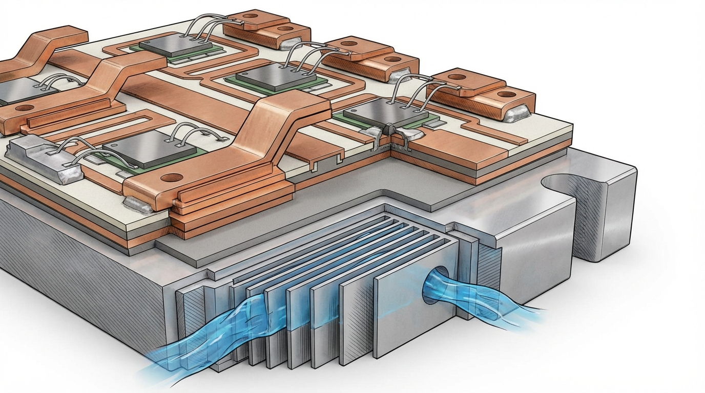
4. From Die to Module: Packaging, Thermal Interfaces, and Reliability
WBG devices realize system‑level benefits only once embedded in robust modules: discrete packages for chargers, half‑bridge and full‑bridge modules for EV traction, multi‑chip RF line‑ups for radar and base stations. Packaging is where semiconductor physics meets copper, ceramics, and thermal grease.
SiC MOSFETs for 800 V EV platforms typically sit in modules that must handle repetitive high dV/dt and dI/dt, wide temperature swings, and mechanical vibrations. GaN devices for data center power supplies run at higher switching frequencies, shrinking magnetics and capacitors but compressing thermal margins in smaller form factors.
4.1 Module Technologies and Emerging Bottlenecks
Key technical features of modern WBG power modules include:
- Substrates and baseplates: Direct‑bonded copper (DBC) or active metal brazed (AMB) substrates, often based on alumina, aluminum nitride, or silicon nitride ceramics, balance thermal conductivity, mechanical robustness, and cost. Si3N4 is gaining share for high‑reliability automotive and rail applications.
- Interconnects: The industry is shifting from traditional aluminum wire bonds to copper wire, copper clips, or sintered silver and copper layers. Analyses referenced in [4] describe cost reductions of roughly 20% in some module families when moving from gold wire bonding to high‑volume copper clip processes, alongside improved current handling and thermal performance.
- Thermal management: Junction‑to‑case thermal resistance remains a primary constraint, especially for compact GaN modules. Figures around 0.5 K/W or lower are often targeted for high‑power automotive modules, demanding careful stacking of die attach, substrate, baseplate, and interface materials.
- Reliability and standards: Automotive‑grade GaN and SiC modules must pass AEC‑Q101/Q102 and extended mission‑profile testing. Grid and aerospace applications impose their own qualification regimes, further lengthening time‑to‑market for new package designs.
Packaging supply chains are geographically more diverse than substrate or epi capacity. Module assembly occurs in North America, Europe, Japan, Southeast Asia, and China. Labor and land cost differentials favor Southeast Asia and parts of China for high‑volume, cost‑sensitive modules, while security‑sensitive or defense‑linked modules often remain in the U.S., Japan, or Europe under controlled supply chains.
Compliance adds friction. U.S. regulations such as the Uyghur Forced Labor Prevention Act have already led to detentions of some electronics imports where polysilicon, metals, or other upstream materials trace to high‑risk regions. Even when WBG module BOMs do not explicitly include those inputs, traceability systems increasingly need to map back through suppliers’ suppliers, adding overhead for sourcing and audit teams.
5. Cross‑Cutting Risks 2024–2033: Geopolitics, Scaling Physics, and ESG
The WBG chain faces three intertwined classes of risk: geopolitical concentration and controls; scaling physics at substrates and epi; and ESG‑driven policy and financing constraints. None of these operate in isolation.
5.1 Geopolitical Concentration and Export Controls
Gallium is structurally the most exposed. With China historically responsible for the overwhelming majority of refined gallium output and Europe, Japan, and the U.S. heavily dependent on imports, the 2023 export license regime was a clear signal. Scenario modeling in [2] and [9] explores tighter regimes from 2025 onward, including volume caps differentiated by country group and explicit end‑use screening for RF and defense applications.
On the device side, U.S. and allied export controls are increasingly attentive to GaN and SiC as enablers for advanced radar, electronic warfare, and hypersonic systems. Proposals often grouped under “BIOSECURE” or similar banners in U.S. legislative discussions contemplate restrictions on sourcing from, or manufacturing in, Chinese fabs for critical‑infrastructure and defense‑adjacent applications. Even if such measures are phased in gradually, they introduce planning uncertainty for OEMs relying on mixed‑geography supply chains.
Russia‑related sanctions further complicate MG‑Si and carbon feedstock flows into Europe, with some SiC precursor streams effectively off‑limits for EU and U.S. buyers since 2022–2023. Arctic or alternative routes often imply longer transit times and higher shipping costs, reshaping relative economics between regional supply options.
5.2 Scaling Physics and Capacity Ramps
Substrate and epi scaling risks differ from the familiar Moore’s Law template. In WBG, higher voltage ratings and current densities often demand more material and higher crystal quality, not less. Moving from 650 V to 1,200 V devices raises requirements on epitaxial thickness, doping uniformity, and defect control, increasing processing time and tool utilization even before diameter scaling.
Industry analyses such as [3] suggest that each new wafer diameter generation for SiC can consume 12–18 months of yield‑learning before stabilizing at high‑volume manufacturing yields. During this window, effective capacity is materially lower than nameplate. Foundries and IDMs frequently prioritize automotive and defense‑linked contracts under allocation, leaving smaller industrial and consumer segments more exposed to shortages or lead‑time spikes.
In WBG, CAPEX alone does not guarantee supply; process maturity and defect learning curves are the real currency of capacity. Large, subsidized fabs can still run “empty” in yield‑adjusted terms if crystal growth, epi, and process integration issues are not solved on schedule.
5.3 ESG, Water, and Carbon Constraints
Upstream, bauxite mining and alumina refining face increasing scrutiny over red mud disposal, water use, and community impacts. Adding gallium recovery to these flows may improve the overall value and critical‑mineral profile of existing assets but does not eliminate underlying ESG concerns. Projects in water‑stressed regions, such as parts of Inner Mongolia, have already been subject to output or expansion constraints linked to local water regulations.
SiC precursors, produced in high‑temperature furnaces, are electricity‑intensive. Where grid mixes are coal‑heavy, SiC embedded emissions can be materially higher than for silicon produced in hydro‑backed regions. As EU and other jurisdictions consider product‑level carbon labeling and border adjustment mechanisms, these upstream profiles begin to matter for downstream device and module acceptance, not only for corporate ESG scoring but for regulatory compliance.
At the fab and module‑assembly level, WBG expansion intersects with local air, water, and waste rules. Nitrides and fluorinated gases used in etch, deposition, and cleaning steps fall under evolving HF, NF3, and F‑gas regulations. Wastewater from polishing and slicing of SiC boules contains fine particulate SiC and metals that require advanced treatment systems. These compliance layers add fixed and variable costs and elongate permitting timelines for new projects.
6. Observed Supply Configurations and Trade‑Offs
The WBG supply chain is not converging on a single optimal configuration. Instead, distinct patterns are emerging, each with its own risk and cost profile.
6.1 Deeply Integrated vs Distributed Models
Some IDMs pursue vertical integration from substrate through module, especially in SiC for EVs and industrial drives. This model internalizes substrate and epi risk but raises capital intensity, tool dependency, and single‑company exposure to process‑yield challenges. It tends to favor companies large enough to amortize high fixed costs across multi‑sector demand.
In parallel, a distributed model persists in which substrate specialists, epi houses, foundries, and outsourced assembly and test (OSAT) providers each handle one link. This configuration can be more flexible and cost‑efficient, but it depends on contract structures, long‑term wafer agreements, and the durability of cross‑border logistics under political stress.
6.2 GaN vs SiC Allocation by End‑Use
Allocations between GaN and SiC are also evolving rather than fixed. Deloitte’s work and other market analyses [2][7] broadly associate SiC with high‑power EV traction, rail, and industrial drives, and GaN with high‑frequency, mid‑power applications such as data center PSUs, consumer fast charging, and RF. Over the next decade, however, vertical GaN progress, combined with packaging and cooling innovation, could push GaN further into roles currently dominated by SiC, especially in regions or segments more constrained on SiC substrate supply.
Conversely, SiC could displace some GaN in automotive on‑board chargers and DC‑DC converters where OEMs and Tier‑1s prefer single‑material platforms for qualification efficiency and long‑term reliability data accumulation.
6.3 Industrial Resilience and Financing Logic
From the standpoint of industrial resilience and operational continuity, WBG fabs, substrate plants, and even key upstream smelters are increasingly treated as critical infrastructure rather than just production assets. Public subsidies, loan guarantees, and long‑term off‑take agreements in the U.S., EU, Japan, and elsewhere are less about financial return optimization and more about ensuring that high‑voltage EV platforms, defense systems, and national grids are not hostage to a single foreign bottleneck.
In practice, this leads to hybrid financing structures. Large SiC programs blend corporate capex with government grants and strategic offtake commitments; gallium recovery expansions attach to broader alumina upgrades justified partly on critical‑mineral security grounds. For risk managers, the key is that these facilities now sit under a different political and regulatory lens than commodity smelters or generic OSAT houses.
7. Conclusion: A Materials‑First View of WBG Power
The WBG revolution is often narrated through device metrics—on‑resistance, breakdown voltage, switching frequency. A materials‑first view tells a different story. It shows how 500 metric tonnes per year of gallium, produced largely as a byproduct in a few bauxite refineries, and a limited number of ultra‑high‑purity SiC boule lines now constrain the trajectory of EVs, AI data centers, and strategic defense systems.
Technical advantage in WBG is increasingly defined not just by who designs the fastest transistor, but by who controls and de‑risks substrate, epi, and module capacity under tightening regulatory and ESG constraints. Choices around integration depth, geographic diversification, and technology roadmaps (GaN vs SiC, 200 mm vs 300 mm) will shape how resilient national and corporate electrification strategies prove to be under stress.
Materials Dispatch continues to track weak signals across this chain—from MOFCOM export filings and USGS gallium data to tool shipment patterns, utility interconnection queues for new fabs, and changes in automotive inverter specifications—that will determine how the WBG supply landscape actually evolves versus headline projections.
Note on Materials Dispatch methodology Materials Dispatch links text monitoring of regulatory and policy sources (including MOFCOM releases and U.S./EU export control updates) with market and capacity data from industry reports and company disclosures. These are cross‑checked against end‑use technical specifications in EV, data center, telecom, and defense systems to understand not only where bottlenecks lie today, but how changes in materials, wafer formats, or packaging will propagate through real industrial architectures.
Sources
- [1] Stratistics Market Research, Compound Semiconductor Foundry Services
- [2] Deloitte, Beyond silicon: GaN and SiC semiconductor technology
- [3] TokenRing article, The power revolution: How GaN and SiC semiconductors are electrifying the AI and EV era
- [4] Global Market Insights, Silicon Carbide Market
- [5] Market Data Forecast, Silicon Carbide Market
- [6] Precedence Research, Power Semiconductor Market
- [7] SkyQuest, GaN and SiC Power Semiconductor Market
- [8] GlobeNewswire, Compound Semiconductor Materials Market
- [9] Discovery Alert, Investment Psychology & Critical Minerals Capital Allocation
- [10] Semiconductor Industry Association, Chip Supply Chain Investments
- USGS, Gallium Statistics and Information
- IEA, Critical Minerals Market Review 2025


